¶ Hydrophones Project
¶ Project presentation
At the Robosub competition, there is around 10 tasks to complete in the TRANSDEC. Two lcoations requise a system to track a sound from a pinger. This pinger works in a frequency range of 25 khz to 40 khz at 5 khz increments. When starting your run, you can choose between selecting a location or having a random location.
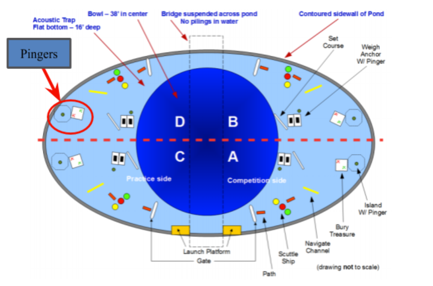
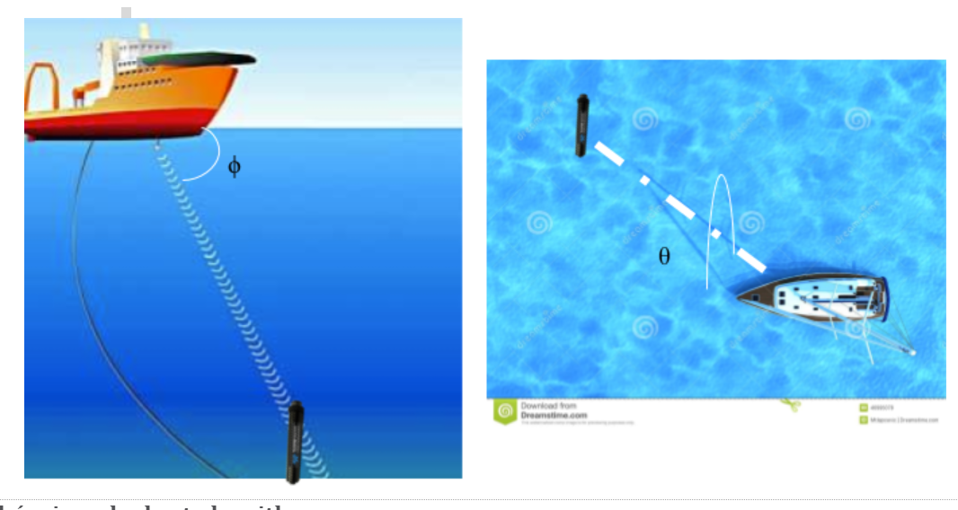
To find these locations, SONIA has designed an hydrophone system for this purpose. In general, the hydrophone are used to calculate the delay between the reception of a ping from the reference to the 3 other hydrophones. With the phase difference, we can get the angle (heading) for the X reference on the submarine and the angle bewteen the X and Y plan and the pinger. These 2 angles are used to navigate at 2 positions. Only the heading would be necessary for the competition, but the system is more reliable with the 2 angles and it is easier to confirm the mouvement of the submarine. Here is a representation of the 2 angles :
The project is divided in 3 parts. The first part is the hydrophones, the second part is the revised hardware and the thrid part is the new firmware.
¶ Hydrophones
Brüel and Kjaer have been sponsoring the team for more than 7 years. They have been helping use with our hydrophone projects. For AUV8, B&K have generously sponsor the team with 5 hydrophones and were able to shorten the length of the cable to 1 meter. For us, it's a great improvement since the cable original length is 6 meters. On AUV7, this was an issue and they had to cut the cable. That made the hydrophones on the previous platform pratically unsuable. To connect the hydrophone to the board, we are using an adapter from the 10-32UNF to BNC.
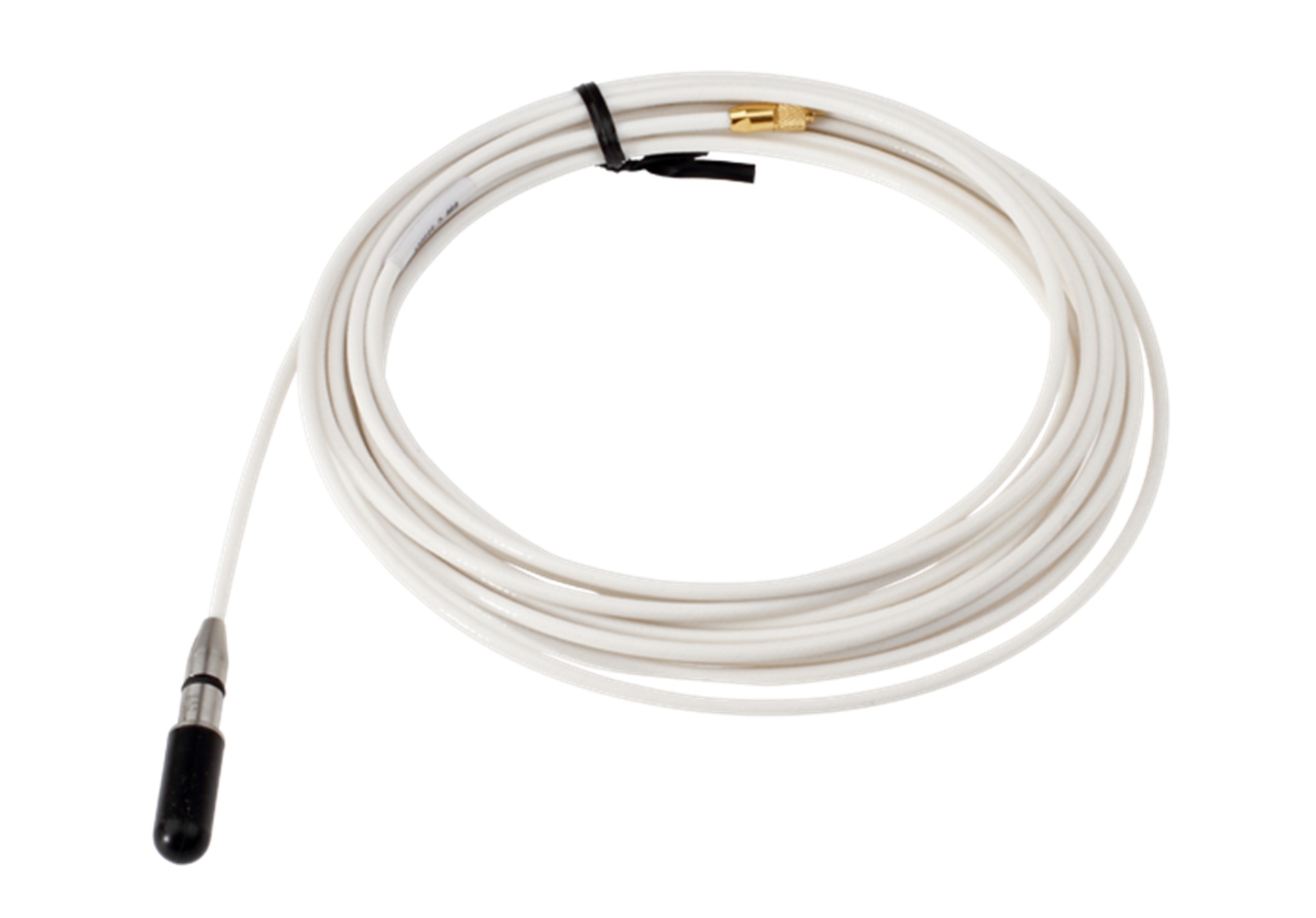
Here is the link for the hydrophones we use : https://www.bksv.com/fr-FR/products/transducers/acoustic/microphones/hydrophones/8103
To simplify the design, the hydrophones are transducers that converts the changes in the water pressure to an electrical signal. It shares some similarities to a piezo sensor.
¶ Hardware design
The hardware design is in 3 parts : FPGA chip, Power and Filters.
¶ Filters
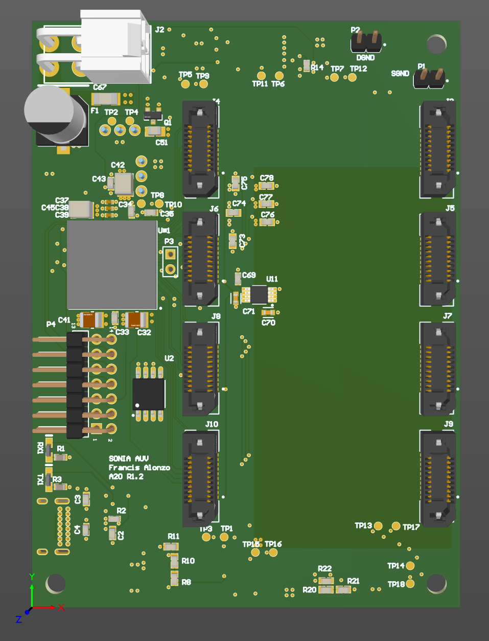
To start with the filters, a desicion was made to isolate them from the noise that can be generated by the DC-DC converters of the board. The filters are now isolated with a separate board that is inserted on the main board. This also makes that all of the channels have the same noise level since they are all identical on the layout and components choice.

The filter works in 3 stages with an ADC. The first stage is the OPA140 high precision, low noise, 11 Mhz JFET op amp. The op amp is set as a charge amplifier and is placed as close as possible from the BNC connector. The second stage is made of filters only. It's a 8th order Chebyshev filter that has been created with the Analog Filter Wizard. Here is the link and the file used to create the filter :
There is no amplification during the filtering stage. The final stage is a programmable gain amplifier. The chip used is the LTC6910-2. The setting can easily be done with 3 GPIO from the FPGA. A step-up is used for the chip since the VCC of the LTC6910-2 is 5V and the IO bank of the XC7S50 is 3.3V. Simulations have been done tob make sure that the amplification and filtering is working. The multiple files can be found on the TEAMS.
¶ Power
Secondly, the Power has been created following the guidelines of the Xilinx documentation. The power tree following has been created with those documentations :
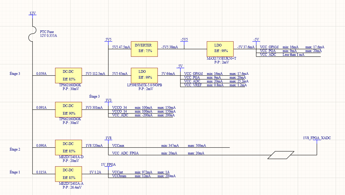
The 1V and 1.8V DC-DC converters haven't been created by ourself to respect the maximum ripple of both voltage supply and to simplify the design. The only drawback is that the space used by the converters are a lot bigger than it would have been if we did ourself. The converters poke out under the board and limit the mechanical mount.
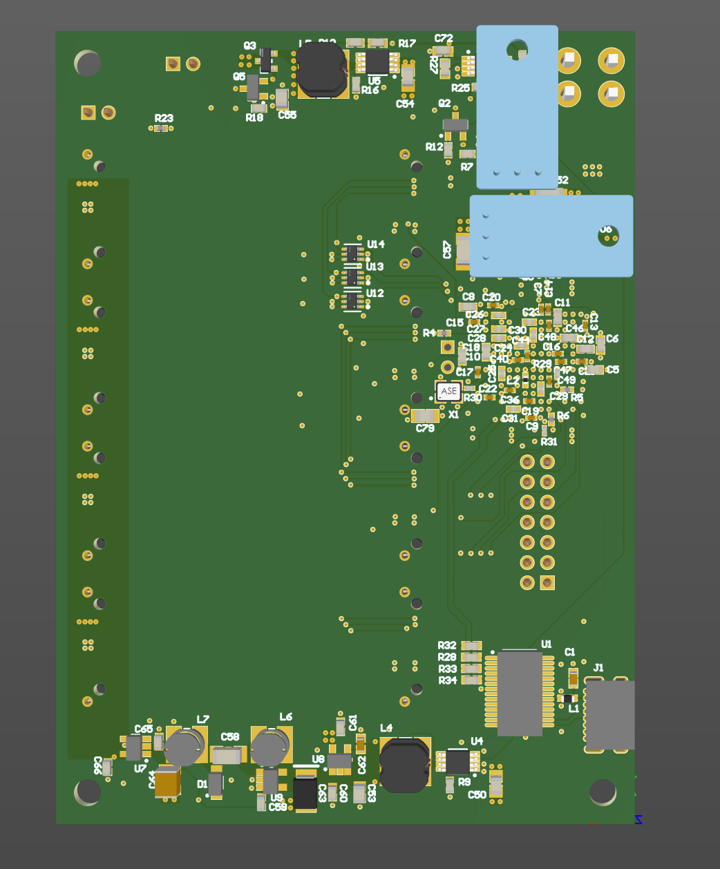
On the PCB design, the 1V, 1.8V and 3.3V are close to the FPGA since these 3 power rails are used directly by the chip. For the 5V and -5V power rails, the converters and LDOs are placed as far as possible from the FPGA without adding any additionnal constraints. It can help for the noise generated, but haven't been tested yet.
¶ FPGA choice
Finally, the FPGA chosen is the XC7S50. It has been chosen by the team of the final project for the calculation of the position / heading of the pinger on the FPGA. The other choice would have been the XC7S25 but the math are too big to be integrated in the chip. Their paper is in the TEAMS.
¶ Firmware design
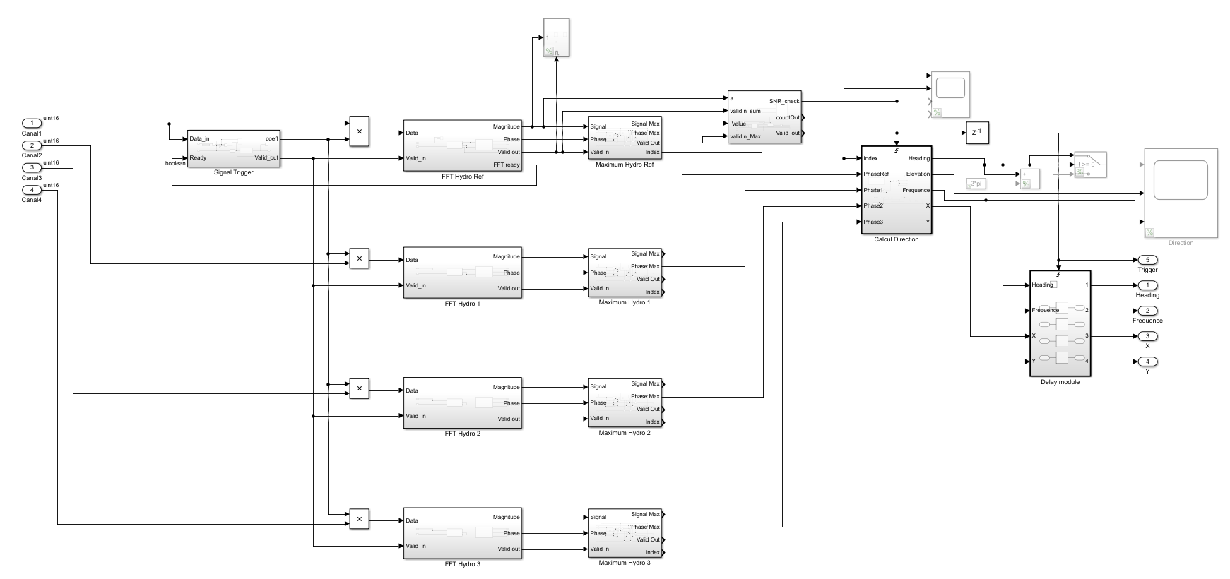
As mentionned above, a team of undergraduate did a final project to calculate the heading and elevation. The project has been done on Simulink. It's using the data from the 4 ADCs as the input and give the frequency, heading and a unit vector as the output. This project can be exported in VHDL with the extension HDL coder of Simulink. There is only one important matrix in the whole project and it can be calculated with the equation following.
(Z with little offset to remove singularity zone)
Here is a picture of the Simulink used for the project. To reopen the project, you will need the simulink project file and the init.m file again in the TEAMS.
¶ Vivado
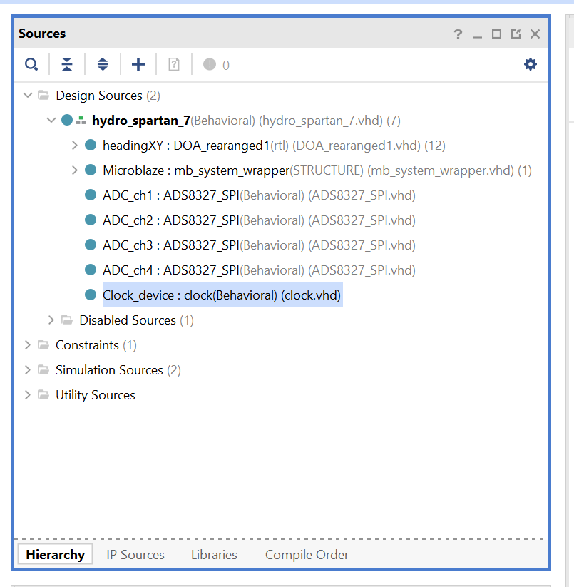
To finish the firmware for the XC7S50, we have used the vivado application (version 2020.2). For our project, there is 2 types of files : the source files and the constraint files. The source files are the files with VHDL code. Most of those files have been generated automatically with the block design of the Microblaze (core). The constraint file gives the pinout of the XC7S50 and the important settings for the programmation of the flash. We will get to those later.
In the project, we are using only a few custom files : the simulink project, the SPI custom driver and a clock divider. Since we use the same ADC as the last revision, we are using the same driver with some slight modifications to the output that where not necessary for the project. The clock divider is required for the SPI driver since the ADC is using a second clock for the conversion time. That clock couldn't be generated with the Microblaze so it had to be created manually.
The block design regenerate most of our files. We use the block design since it's easier to work with and we don't make any mistake on our connections. Here is the block design used on the developpement board (it's the same as the main project) :
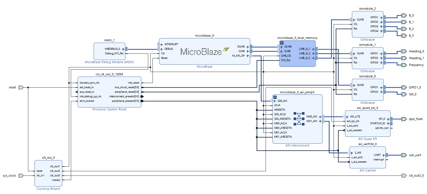
Here is a brief explanation of the design. The Microblaze block create most of the blocks and the connection are made automactically. For the clock, we use a 100 Mhz input clock and 3 outputs : 10 Mhz (limitation from the simulink project) for the overall of the fpga, 50 Mhz for the Quad SPI flash and 25.8 Mhz for the external clock divider. The 10 Mhz is used by the microblaze and is sent to be used externally of the block design. We use the Quad SPI block to program on the flash that we added on the new revision (MX25L3233F). The connection are made external of the block design. Then, the UART block is a simple addition to communicate with a console. Finally, we use 3 IO_Module to send and recevier data from the C application. The IO_Module 1 & 2 are used for the data and the IO Module 0 is used for general settings for the data transfert and to send a signal when the heading has been calculated.
The final file in VHDL is the top level file. This file regroups all the previously mentionned files to create a functionning firmware. It directly connects to the constraint file since it connects the pinout with the right signals. There is some simple process that are required to the right function of the firmware. Here is the mapping of the Microblaze with signal and direct pinout (UART & SPI are an example):
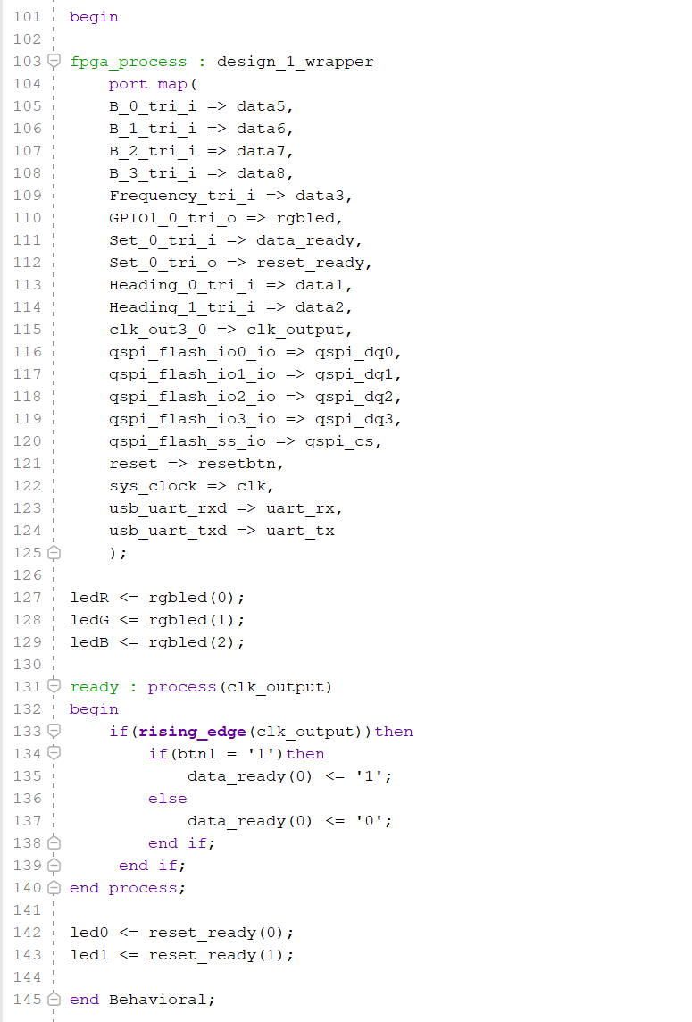
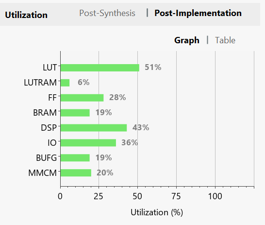
With the normal work flow of Vivado, we run the synthesis and implementation and if we don't get any errors, we can generate the Bitstream. The Bitstream is used to create the C application that is gonna run over the VDHL code. It wil create a .XSA file. This C application is programmed with VITIS. The implementation done with the XC7S50 has produced the following results :
¶ VITIS
Now, we need to write the code to interface between the hardware of the FPGA and the submarine. To transfer the data between the hardware and C, we use the IO Module, as mentionned previously. These modules have a set adress on the FPGA and are easily accessible with the generated address. To read the data on the onboard computer, we use the terminal and some regular expressions to remove the use of a custom UART.
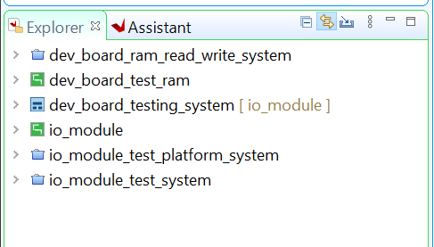
Firstly, we need to create the board that is going to be used by the C program. You will need to create a new application. It creates a custom board and a new project. If you modify the VIVADO code, you don't need to recreate a new application. You can update the board with your new .XSA file. When creating your application, a good pratice is to use a template from VITIS so most of the initialisation of the chip is already programmed. With this step done, you should have this result :
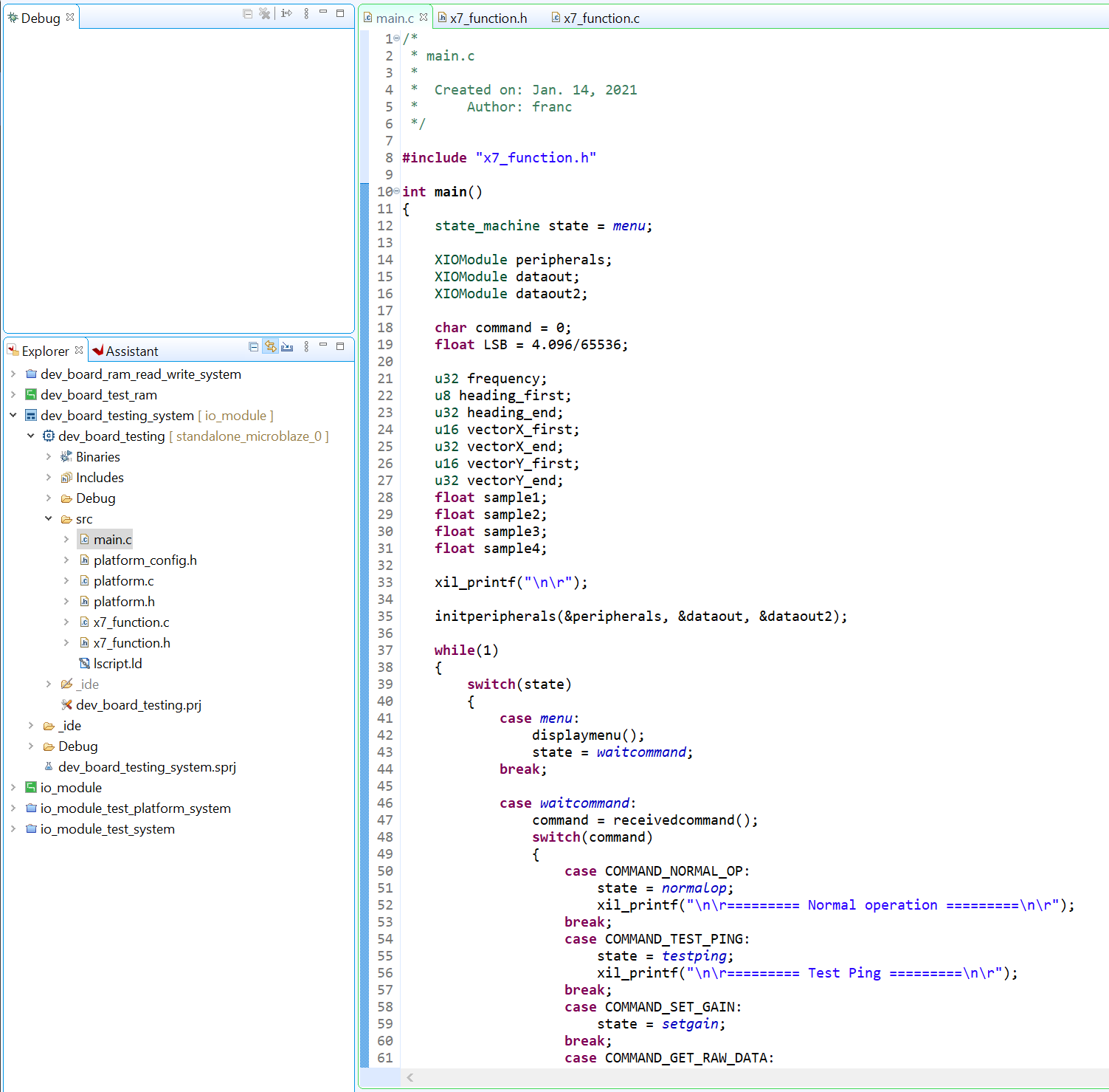
Next, you can write the code to run your program in a new file called main.c. To make sure you don't have any issue, remove the file from the template that had the main program in it. In the main, we have a infinite while loop and a switch case that is used for the menu. A better program would be have an interrupt to stop the program. To reduce the length of the main.c file, all the support function for the menu are placed in an other file and included in the primary file. Here is a part of the main program :
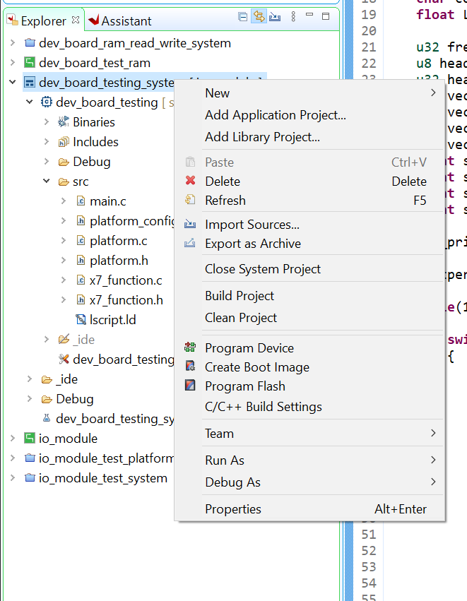
The only thing left to do on VITIS is to try the code written. To program the new version of the code, the application (blue icon on the explorer) needs to be built. This can be done by right clicking on the application.
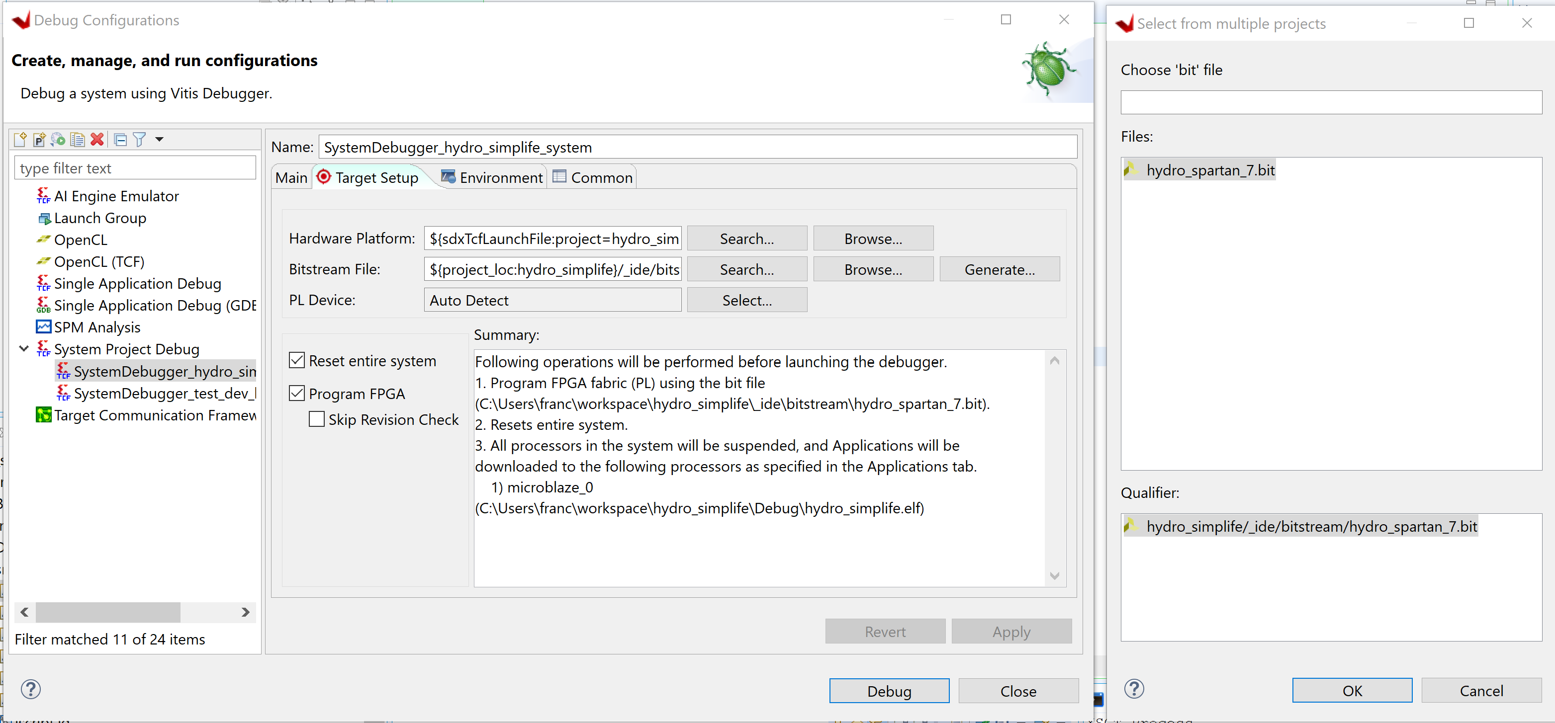
Then, you can again right click on the application and select the Debug as or Run as command. The debug command will allow you to place breakpoints in your code to test it. You might need to select the right bitstream file in the debug configuration if you get any warnings during the debug session.
¶ Programming the flash
When you are done with your application, we will need to go back in VIVADO to program the flash on the hydrophone main board. You will need the .elf file on VITIS. Make sure that the file is up to date on the latest code you wrote. The file can be updated with the build command. A good practice is to clean your project and then rebuild it to get a fresh version.
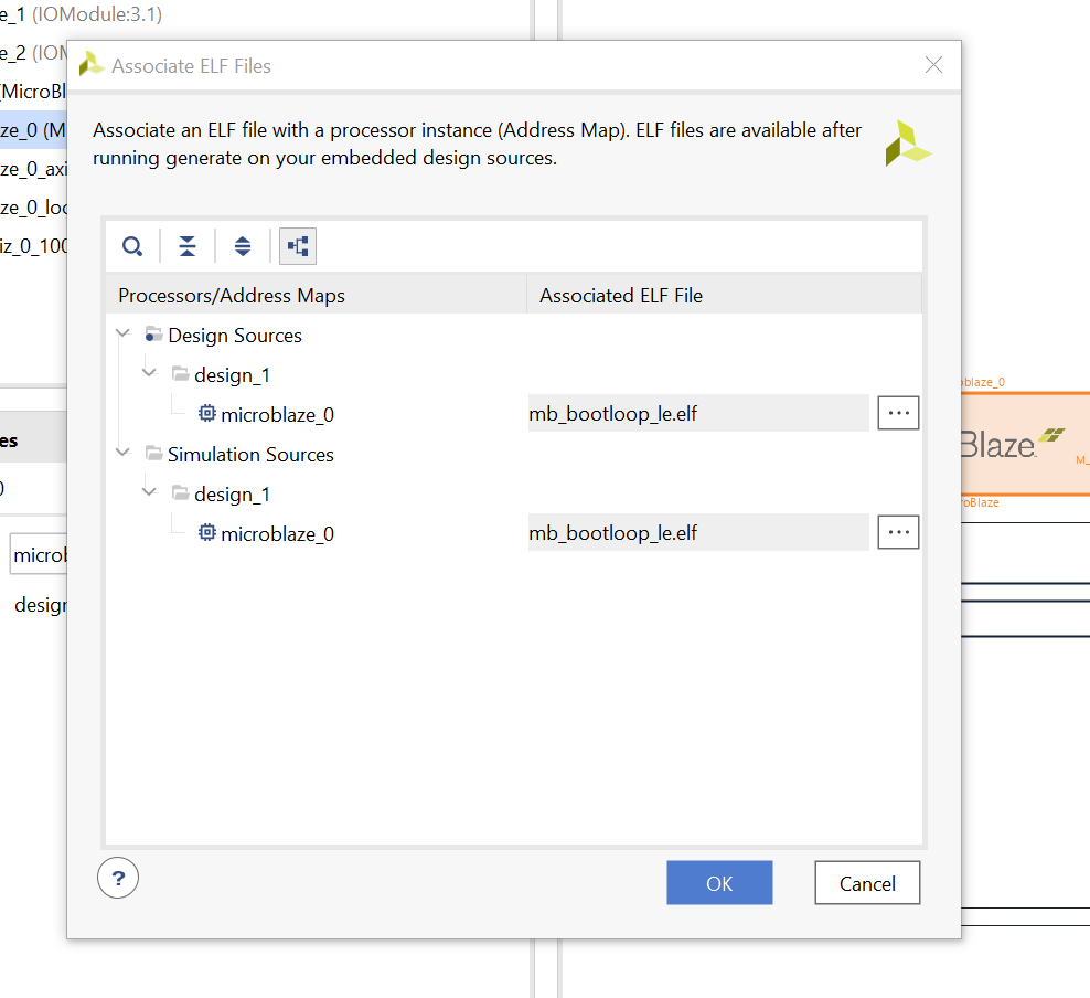
This file has to be placed 2 places. The first place is in the Microblaze block from the block design. By clikcing on the block, you can go on the setting Associate elf file. Still in the block design, make sure that the clock for the SPI is over 33 Mhz. After, add the .elf file into the constraints of the project.
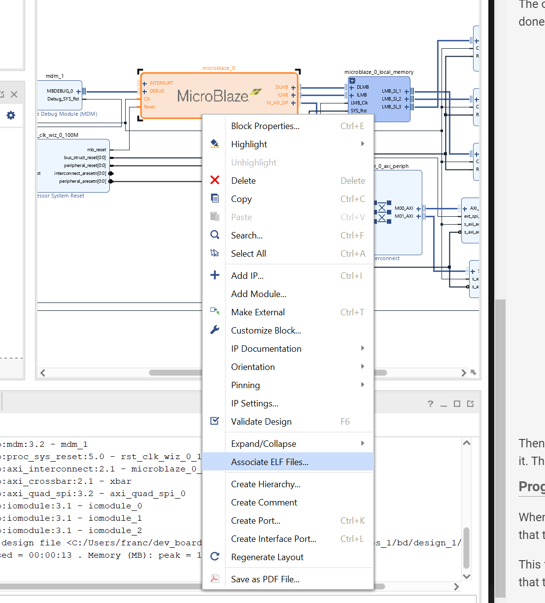
Here, you just need to change the source .elf file.
Before, writing a new bitstream to be flash. We need to change some settings. In the general settings, activate the generation of the bin file on the Bitstream section. Also, in the contraints file, add the following properties to suit the Quad SPI flashing (all lines with current design in [ ]).
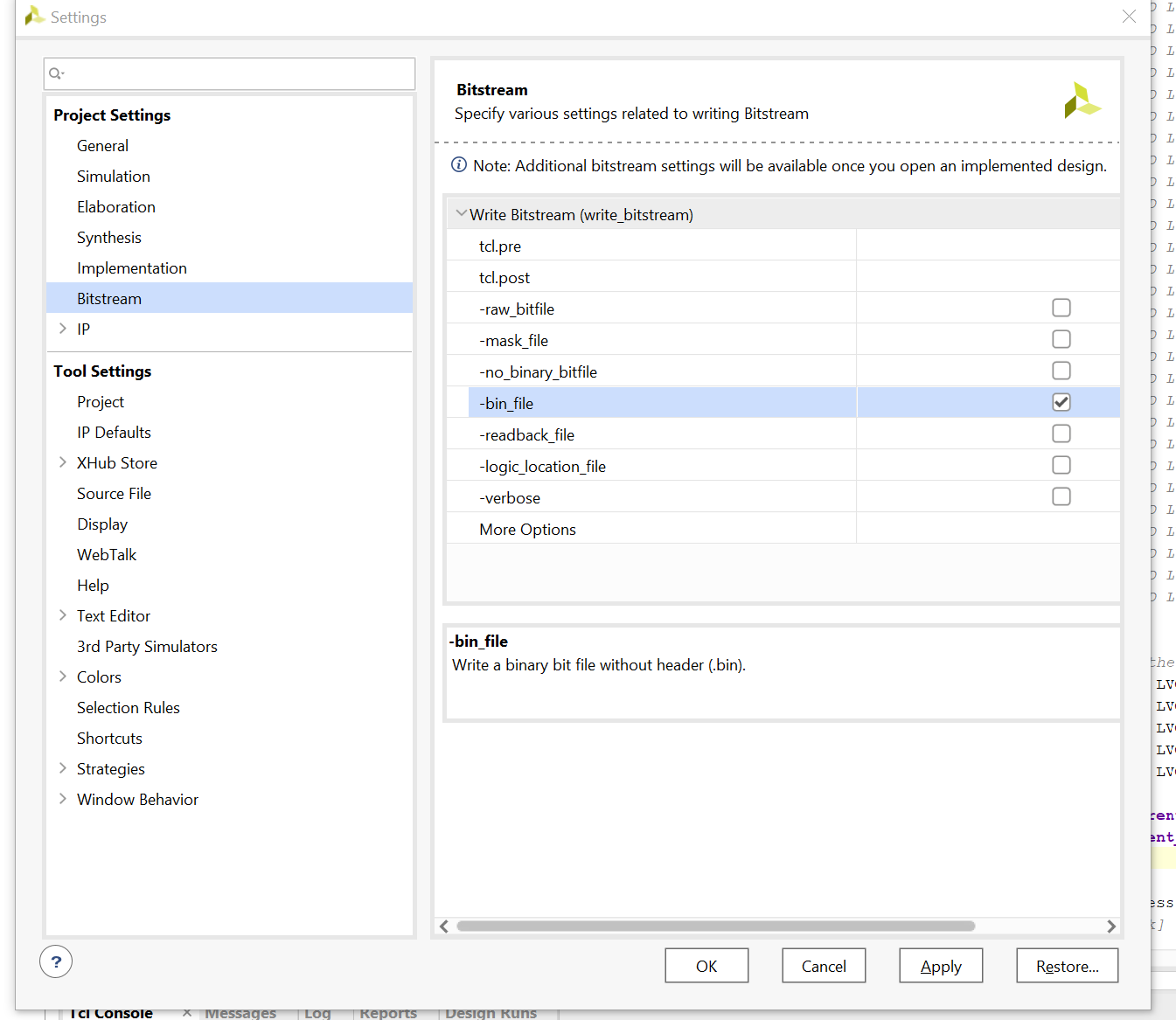
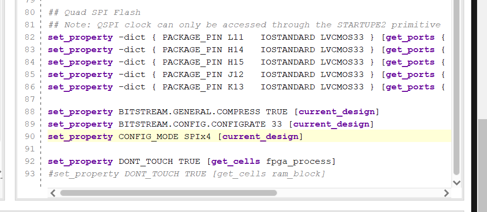
When all these settings are done, you can regenerate a Bitstream. It will now include the .elf file with it. Finally, it's time to program the flash on the board. To do that, you need to open the hardware manager and connect to the board itself in JTAG. The FPGA used should appear.
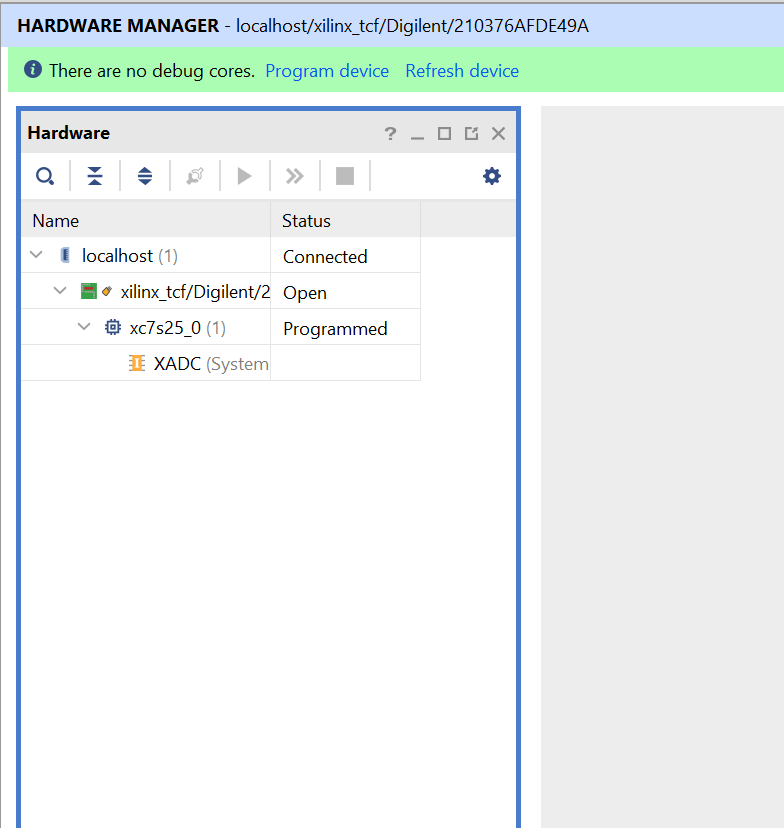
By doing a right click on the chip name, a menu will appear and you need to select the button Add configuration memory device. A window will open asking you the chip of the memory. For the hydrophones, we use the MX25L3233F from Macronix.
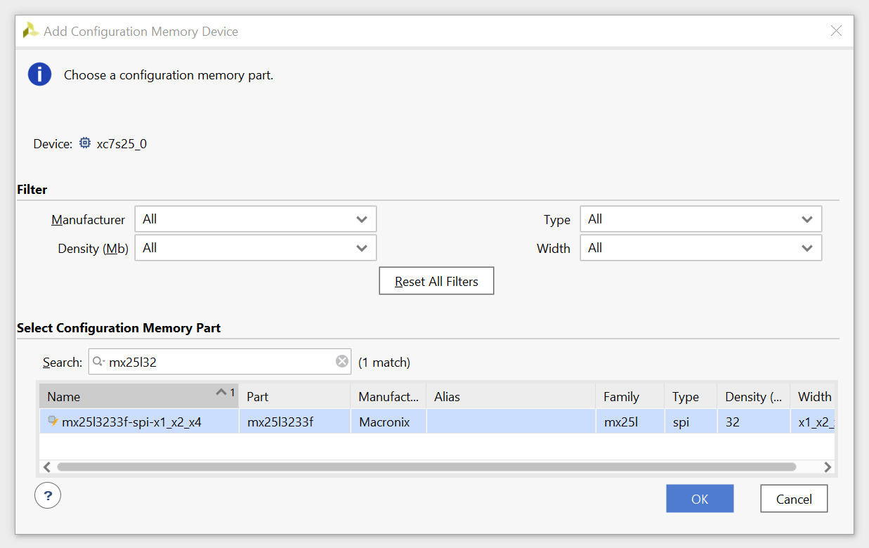
After selecting it, you can accept to program it now. The bin file generated with the bitstream is going to be needed at that point. Right click on the memory device and select the option Program Configuration Memory Device Select the required bin file created and leave the rest of the settings to the default.
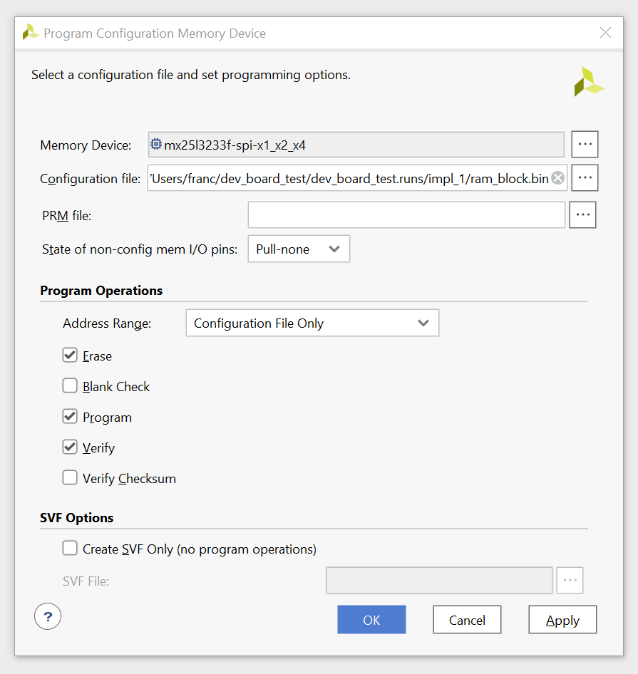
When the program is complete, the board is ready to go. To verify that the flash programming worked, reboot the board and check that it's doing the right behavior.
¶ Second revision
There are few changes where made on the main board to improve it.
We have changed the reset switch for something easier to press on. The switch on the revision #1 was impossible to press.
We had some software issue since we had a 100 MHz crystal instead of the 12 MHz crystal as on the developpement board.
We also change the UART communication with a tri-state buffer has been added in order to limit leakage throught the FPGA when only the usb powered on. Also, we have implemented a reset of the fpga when the port is opened on the USB on the FT232R. This can be toogled with a jumper if the board needs to be programmed without the USB connected.
Some 22 ohms have been added the SPI clocks to reduce the reflexions produced with the 25 MHz clock. They should have been there since the first revision.
¶ Issues
There is a few issues with the second revision of the hydrophone main board.
First of all, the 12 MHz clock footprint was too big for the initial part chosen. An other oscillator had to be chosen to work on the footprint. The signal of the 12 MHz clock wasn't as clean as excepted. An extremely agressive 15 MHz RC low-pass filter has been added to reduce the ringing.
Secondly, the mosfet used for the power sequencer didn't have the right footprint. The Drain and Source were inverted. The mofset was been solder in a way to make them work but the solution isn't optimal.
Finally, there is a weird behavior on the board. When the power sequencer gets to the last power rails, there is a component that makes a clicking noise. It wasn't possible to found the exact source but it could be related to an high inrush current to charge all the capacitor or a short somewhere on the 3V3.
¶ Software Improvements
The software is still in developpement but you can consult the Github page of the project : Hydrophones Github repo
As 2021-05-30, the SPI communication is working by increasing the SPI clock from 5 MHz to 25 MHz but there is a adjustement missing in the code to get the heading and elevation.
As 2021-06-28, the SPI and ADC are working with some unit testing. We have applied a voltage directly to the ADC and the value is correct on the screen output. The code for the heading and elevation has been changed since it wasn't considering that the data from ADC was only at 256kHz and not 10MHz. The generated code was taking a new sample at each rising edge of the 10 MHz clock. With the changes made, the code doesn't fit anymore in the XC7S25. The code will be tested with the second board revision.
As 2021-09-20, the conversion clock for the ADC is now generated by a PLL to ensure that the frequency is exaclty 256 kHZ. The previous method gave a frequency of 256.4 kHz and now it's at 256.003 kHz. Also, the Matlab code generation has been changed to remove the adaptive pipeline and to add the Balance delays which is critical for an FPGA implementation.
As 2022-02-22, the general program is working but not tested during a pool to see if the DOA is accurate. The UART was causing issues. After entering a few commands, the buffer for the UART was filling up or something like that and the menu was broken. We could enter a new command anymore and the board needed to be power cycled. To solve this issue, the UartLite IP core was used instead of only using STDIN and STDOUT. The STDOUT is still use to print data but the STDIN has been replaced by the UartLite API. Also, the FIFOs for the receive and send are being reseted each time that the menu is displayed. We havent seen the issue after entering commands repetitively for 5 mins.
¶ How to connect to the hydrophones board
Here is the link for a page that shows how to use the hydrophone board when connected directly in a computer : Connection and Use Hydrophones
¶ Useful links
¶ Hadware
- ADC datasheet
- Spartan 7 Config Documentation
- Developpement Board Cmod S7 Documentation
- Pinger ALP-365
¶ VHDL
¶ Vivado
- Microblaze IP
- Vivado Tutorial
- DONT-TOUCH for constraint files
- Modify BRAM size
- Crossing Clock Domains
- FIFO Documentation
- Logic Debug
- Removing all missing files
¶ Vitis
- SDK to Vitis
- Developpement with Vitis
- Flashing a Microblaze Program
- UartLite API
- Vitis Drivers Github
By : Francis Alonzo
Date : 2022-02-21